Sharp meets flat in tunable 2D material
A Rice University lab wants its products to look sharp, even at the nanoscale. Its latest creation is right on target.
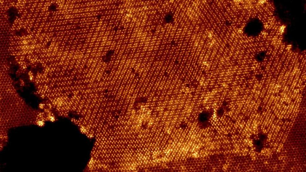
The Rice lab of materials scientist Pulickel Ajayan has created unique two-dimensional flakes with two distinct personalities: molybdenum diselenide on one side of a sharp divide with rhenium diselenide on the other.
From all appearances, the two-toned material likes it that way, growing naturally -- though under tight conditions -- in a chemical vapor deposition furnace.
The material is a 2D transition metal dichalcogenide heterostructure, a crystal with more than one chemical component. That's not unusual in itself, but the sharp zigzag boundary between elements in the material reported in the American Chemical Society journal Nano Letters is unique.
Dichalcogenides are semiconductors that incorporate transition metals and chalcogens. They're a promising component for optoelectronic applications like solar cells, photodetectors and sensing devices. Lead author Amey Apte, a Rice graduate student, said they may also be suitable materials for quantum computing or neuromorphic computing, which emulates the structure of the human brain.
Apte said well-known, atomically flat molybdenum-tungsten dichalcogenide heterostructures can be more alloy-like, with diffuse boundaries between their crystal domains. However, the new material -- technically, 2H MoSe2-1T' ReSe2 -- has atomically sharp interfaces that gives it a smaller electronic band gap than other dichalcogenides.
"Instead of having one unique band gap based on the composition of an alloy, we can tune the band gap in this material in a very controllable way," Apte said. "The strong dissimilarity between two adjacent atomically thin domains opens up new avenues." He said the range of voltages likely spans from 1.5 to 2.5 electron volts.
Growing the materials reliably involved the creation of a phase diagram that laid out how each parameter -- the balance of chemical gas precursor, the temperature and the time -- affects the process. Rice graduate student and co-author Sandhya Susarla said the diagram serves as a road map for manufacturers.
"The biggest issue in these 2D materials has been that they're not very reproducible," she said. "They're very sensitive to a lot of parameters, because the process is kinetically controlled.
"But our process is scalable because it's thermodynamically controlled," Susarla said. "Manufacturers don't have a lot of parameters to look at. They just have to look at the phase diagram, control the composition and they will get the product every time."
The researchers think they can gain further control of the material's form by tailoring the substrate for epitaxial growth. Having the atoms fall into place in accordance with the surface's own atomic arrangement would allow for far more customization.
Story Source:
Materials provided by Rice University. Note: Content may be edited for style and length.
Journal Reference:
- Amey Apte, Aravind Krishnamoorthy, Jordan A. Hachtel, Sandhya Susarla, Jongwon Yoon, Lucas M. Sassi, Palash Bharadwaj, James M. Tour, Juan Carlos Idrobo, Rajiv K. Kalia, Aiichiro Nakano, Priya Vashishta, Chandra Sekhar Tiwary, Pulickel M. Ajayan. Two-Dimensional Lateral Epitaxy of 2H (MoSe2)–1T′ (ReSe2) Phases. Nano Letters, 2019; DOI: 10.1021/acs.nanolett.9b02476